with a co2 laser you can basicly just expose the whole board and remove the unwanted soldermask.
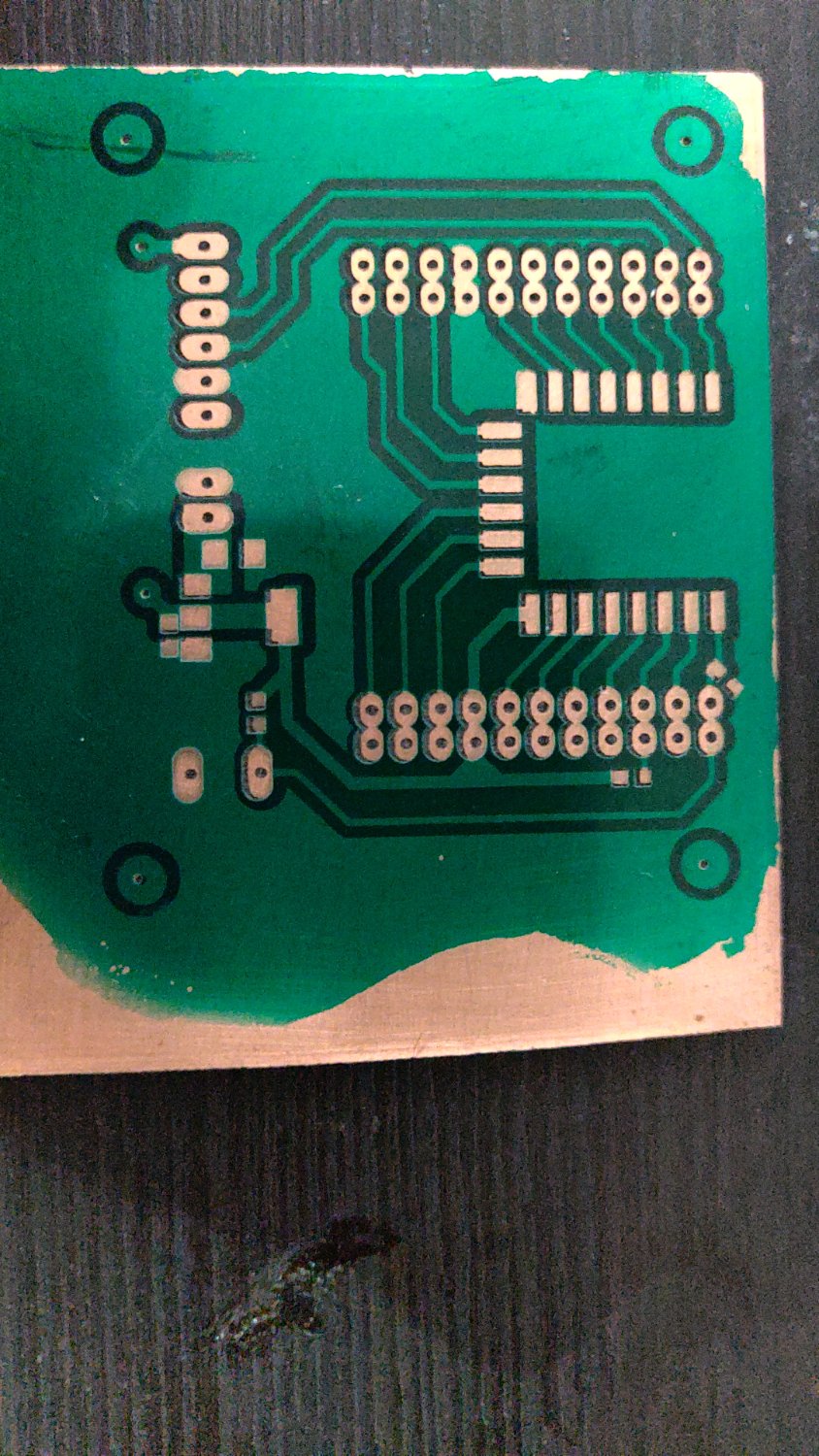
edit: i accidently moved the rig, that's why it's a bit offset.
Projects, pictures, industry discussions and news about electronic engineering & component-level electronic circuits.
1: Be nice.
2: Be on-topic (eg: Electronic, not electrical).
3: No commercial stuff, buying, selling or valuations.
4: No circuit design or repair, tools or component questions.
5: No excessively promoting your own sites, social media, videos etc.
Ask questions in https://discuss.tchncs.de/c/askelectronics
with a co2 laser you can basicly just expose the whole board and remove the unwanted soldermask.
edit: i accidently moved the rig, that's why it's a bit offset.
It works as well with a 450nm diode laser. About 1W worth of laser power will ablate soldermask as well but you risk burning off really small pads because they cannot really dissipate heat anymore. Especially NC pads tend to burn off. I've tried it and it works reasonably well by doing the drilling as the last step.
450nm is unfortunately not good enough to cure soldermask, 405nm is much more effective.
Photolithography is so satisfying to watch. Thanks for sharing.